Silicon IP Cores
MD5
Message Digest Algorithm Processor
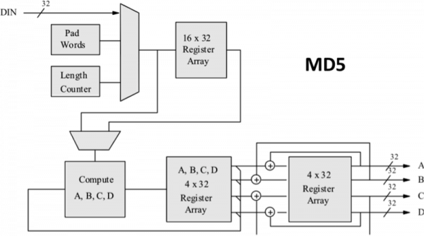
The MD5 encryption IP core is a fully compliant hardware implementation of the Message Digest Algorithm MD5, suitable for a variety of applications. It computes a 120-bit message digest for messages of up to (264 – 1) bits.
The MD5 algorithm is an improved version of the MD4, created by Professor Ronald L. Rivest of MIT, and is closely modeled after that algorithm. It operates on message blocks of 512 bits for which a 128-bit (4 x 32-bit words) digest is produced. Corresponding 32-bit words of the digest from consecutive message blocks are added to each other to form the message of the whole message.
The MD5 core is a fully synchronous design and has been evaluated in a variety of technologies. It is available optimized for ASICs or FPGAs.
The MD5 core has been robustly verified and is silicon-proven.
The process starts with the first message block of sixteen words being clocked into the core. The INIT signal is asserted at the start of each message. The MD5 core is ready to accept data when REQ is asserted.
Each 32-bit word is clocked into the core on the rising edge of CLK when ACK is asserted. After a block of 16 words has been input, REQ is deasserted as the MD5 core computes the message digest. After another 49 clock cycles, the message digest for that 16 word block is computed and REQ is asserted again to indicate that more words can be clocked in.
The standard specifies that the maximum number of bits in the message is 264 - 1. Therefore the maximum number of 32-bit words that can be clocked in is 259 - 1. The core can cope with any number of words up to 259 - 1 being input.
The LAST signal is asserted when clocking in the last word. At least one pad, and two length words need to be added to the end of the message as part of the MD5 calculation.
Note that the BYTE signal is considered valid and sampled by the core when the LAST signal is high. This signal is used by the core to determine how many bytes in the last word are part of the input data.
If the total number of input words plus three is not a multiple of 16, the core adds additional pad bytes to calculate the message digest as specified in the standard.
The two Length words that contain the bit-length of the original message are also added by the core.
The 160-bit message digest is output on A, B, C, D when READY is asserted.
The core has been verified through extensive synthesis, place and route and simulation runs. It has also been embedded in several products, and is proven in FPGA technologies.
Support
The core as delivered is warranted against defects for ninety days from purchase. Thirty days of phone and email technical support are included, starting with the first interaction. Additional maintenance and support options are available.
Deliverables
The core is available in ASIC (RTL) or FPGA (netlist) forms, and includes everything required for successful implementation. The ASIC version includes:
- HDL RTL source
- Sophisticated HDL Testbench (self checking)
- C Model & test vector generator
- Simulation script, vectors & expected results
- Synthesis script
- User documentation
The MD5 can be mapped to any ASIC technology. The following are sample ASIC pre-layout results reported from synthesis with a silicon vendor design kit under typical conditions, with all core I/Os assumed to be routed on-chip. The provided figures do not represent the higher speed or smaller area for the core. Please contact CAST to get characterization data for your target configuration and technology.
|
ASIC Technology |
Number of eq. gates |
Fmax (MHz) |
Throughput (Gbps) |
|---|---|---|---|
|
TSMC 40nm
|
25,160
|
600
|
4.726
|
|
TSMC 28nm HMP
|
12,279
|
800
|
6.302
|
|
TSMC 16nm
|
14,467
|
1,000
|
7.877
|
The MD5 can be mapped to any Altera FPGA device (provided sufficient silicon resources are available). The following are sample results with all core I/Os assumed to be routed on-chip. The provided figures do not represent the higher speed or smaller area for the core. Please contact CAST to get characterization data for your target configuration and technology.
| Family | Logic | RAM bits | Freq. (MHz) |
Throughput (Mbps) |
|---|---|---|---|---|
| MAX 10 (-7) | 1,751 LEs | 0 | 75 | 591 |
| Arria 10 GX (-1) | 719 ALMs | 0 | 125 | 895 |
| Stratix V (-3) | 691 ALMs | 0 | 200 | 1,575 |
| Stratix V (-1) | 689 ALMs | 0 | 225 | 1,772 |
The MD5 can be mapped to any AMD FPGA device (provided sufficient silicon resources are available). The following are sample results, with all core I/Os assumed to be routed on-chip. The provided figures do not represent the higher speed or smaller area for the core. Please contact CAST to get characterization data for your target configuration and technology.
| Family | LUTs | BRAMs | Freq.(MHz) | Throughput (Gbps) |
|---|---|---|---|---|
| Virtex 7 (-3) | 680 | 0 | 300 | 2.363 |
| Virtex UltraScale (-3) | 697 | 0 | 350 | 2.757 |
| Kintex UltraScale+ (-3) | 730 | 0 | 500 | 3.938 |
| Versal (-2) | 661 | 0 | 300 | 2.363 |
Engineered by Ocean Logic.
Features List
- RFC 1321 compliant
- Suitable for data authentication applications
- Maximum message length is 264 - 1
- Simple, fully synchronous, reusable design
- Available as fully functional and synthesizable VHDL or Verilog, or as a netlist for popular programmable devices
- Complete deliverables include test benches, C model and test vector generator


